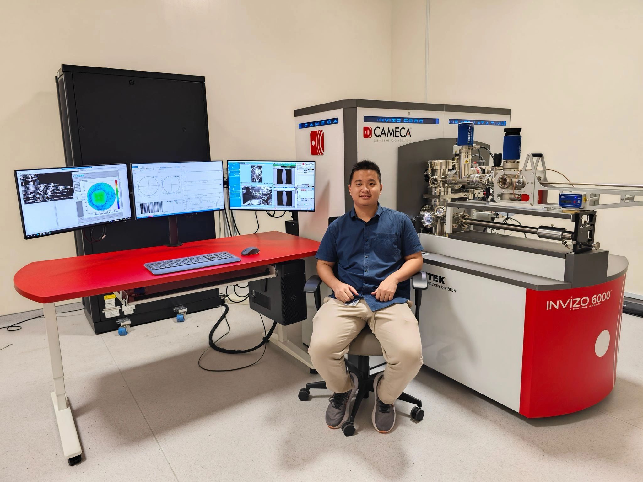
Probing atoms...
The 3D atom probe is a near-atomic resolution materials characterization method that works by evaporating a really tiny (we're talking about <100 nm here) needle and reconstructing the evaporated mass via time-of-flight mass spectroscopy to get beautiful volumes.


Atom probe
Schematic of the atom probe.

Atom probe specimen
SE micrograph of atom probe specimen.
Ni-based superalloys
Understanding γ'-phase formation superalloys processed with different parameters.
Field of view = 165 nm (left), 80 nm (right).
Transistor Devices
Complex structures of transistor devices.
Field of view = 70 nm.
Oxidized metal surface
Understanding chemistry of oxide layer formed on top of metal/alloy surfaces.
Field of view = 50 nm.
Dislocations in metals
Dislocations are commonly marked by some elemental segregation in complex alloys.
Field of view = 90 nm.
Layered Thin Films
Multilayered thin films are common among advanced semiconductor applications.
This website uses cookies.
We use cookies to analyze website traffic and optimize your website experience. By accepting our use of cookies, your data will be aggregated with all other user data.